EcoSys Updates
Why Abatement Systems Are Critical to Semiconductor Manufacturing
12 February 2026
Share this article
EcoSys (Malaysia) Berhad has been developing and manufacturing abatement systems since acquiring the CDO, Vector, Marathon, and Guardian product lines in 2011. As semiconductor manufacturers face tightening environmental regulations across Asia, Europe, and the United States, abatement systems have become a non-negotiable part of wafer fabrication operations.
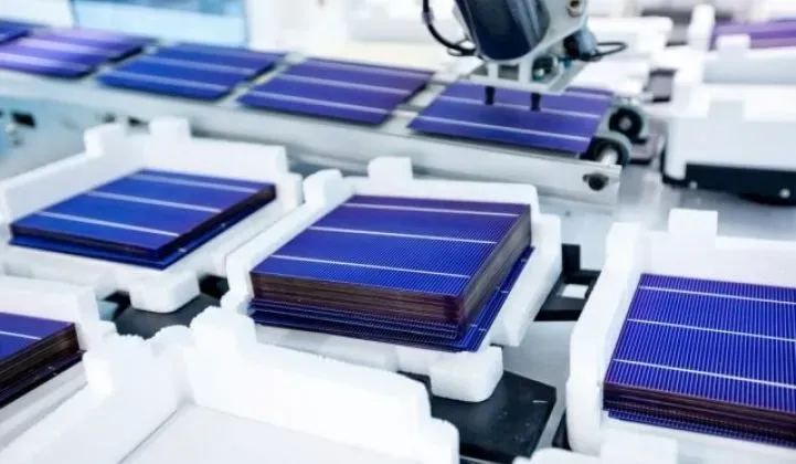
What Happens Inside a Wafer Fab
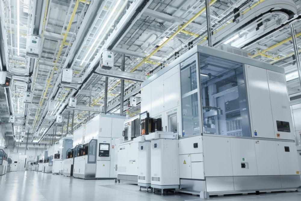
Front-end semiconductor manufacturing involves highly complex processes, including etching, chemical vapour deposition, and chamber cleaning. These processes generate a wide range of hazardous byproducts that must be managed before release. Left unmanaged, these byproducts pose serious risks to personnel, equipment, and the surrounding environment.
The Gases That Need to Be Managed
The gases generated during wafer fabrication fall into several categories, each requiring a different treatment approach. Acidic gases include hydrogen fluoride, hydrogen chloride, sulfuric acid, and nitric acid. Toxic gases include phosphine, arsine, silane, and ozone. Processes also generate organic compounds, fine particulate matter, and greenhouse gases such as carbon tetrafluoride, sulphur hexafluoride, and nitrogen trifluoride. Each gas behaves differently and must be treated accordingly.
How Abatement Systems Work
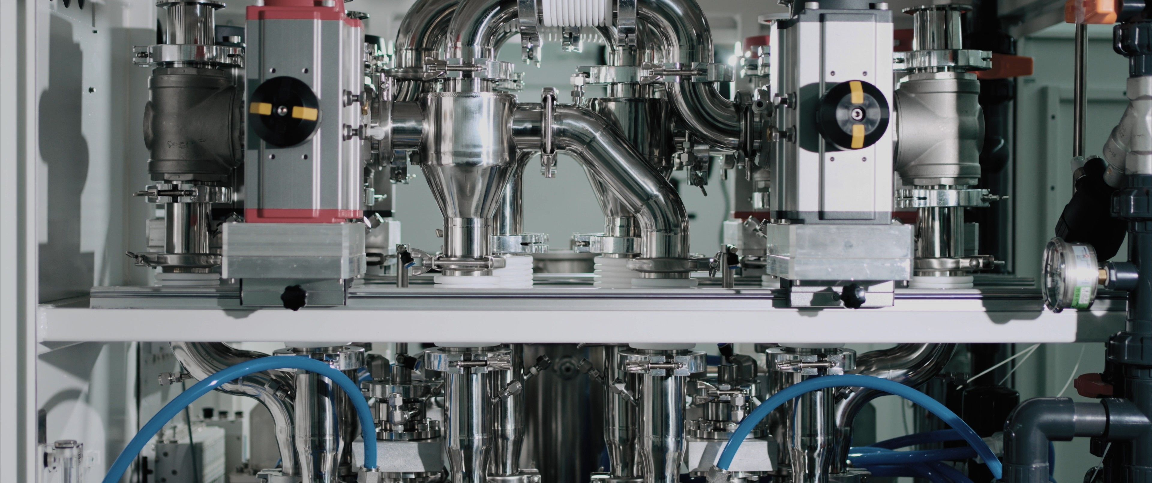
Abatement systems capture, treat, and neutralise harmful gases at the point of generation before they are released into the environment. Treatment methods include dry scrubbing technologies such as thermal oxidation, combustion, plasma, and catalytic oxidation, as well as wet scrubbing and combinations of these methods depending on the gas chemistry involved.
In a typical dry-wet scrubbing system, contaminated gases are first exposed to high-temperature combustion or plasma to decompose harmful compounds. The decomposed gases then pass through multiple stages of wet scrubbing where water captures particles and water-soluble gases before the treated gas is safely discharged.
The Regulatory Drivers
Abatement is required to comply with strict emissions regulations in every major semiconductor manufacturing market. Regulations such as the US Environmental Protection Agency's emission control measures and the European Union's REACH framework are driving manufacturers to invest in more advanced abatement technologies. Beyond compliance, abatement systems also support manufacturers' net zero commitments by reducing Scope 1 and Scope 2 greenhouse gas emissions.
EcoSys's Approach
EcoSys has been developing and manufacturing abatement systems since 2011. Since 2015, EcoSys has invested continuously in R&D to enhance its product lines and develop new models incorporating microwave plasma technology. EcoSys holds 44 patents and 36 trademarks covering the proprietary technologies and branding of its abatement systems, serving customers across 10 countries.


ECOSYS (MALAYSIA) BERHAD
25, Lorong Beringin 2,
Taman Industri Beringin,
14100 Simpang Ampat,
Pulau Pinang
Ultra High Purity (UHP)
© @ 2026 ECOSYS (MALAYSIA) BERHAD 202301024280 (1518203-H). All Rights Reserved. Powered by Orangesoft Web Design